Tem Microscope How It Works ?
A transmission electron microscope (TEM) works by passing a beam of electrons through a thin sample, which interacts with the electrons and scatters them in various directions. The scattered electrons are then focused onto a fluorescent screen or detector, which produces an image of the sample.
The electron beam is generated by an electron gun, which accelerates electrons using an electric field and focuses them into a narrow beam using magnetic lenses. The beam is then directed towards the sample using a series of electromagnetic lenses.
As the electrons pass through the sample, they interact with the atoms and molecules in the material, causing them to scatter and diffract the electrons. This scattering and diffraction produces a complex pattern of electrons, which is then collected by the detector and used to create an image of the sample.
TEMs are capable of producing extremely high-resolution images, with the ability to resolve individual atoms and molecules. They are widely used in materials science, biology, and other fields to study the structure and properties of materials at the nanoscale.
1、 Electron beam generation

TEM microscope, also known as Transmission Electron Microscope, is a powerful tool used to study the internal structure of materials at the atomic level. It works by passing a beam of electrons through a thin sample, which interacts with the atoms in the sample and produces an image on a screen.
Electron beam generation is a crucial component of TEM microscope operation. The electron beam is generated by an electron gun, which uses a heated filament to emit electrons. These electrons are then accelerated by an electric field and focused into a narrow beam by a series of electromagnetic lenses.
The latest point of view on electron beam generation in TEM microscopy is the development of aberration-corrected electron optics. This technology allows for higher resolution imaging by correcting for aberrations in the electron beam caused by imperfections in the lenses. Aberration correction has enabled researchers to achieve sub-angstrom resolution in TEM imaging, allowing for the visualization of individual atoms and their arrangements in materials.
In summary, TEM microscopy works by passing an electron beam through a thin sample, and electron beam generation is a critical component of the process. The latest development in electron beam generation is aberration correction, which has enabled higher resolution imaging and the visualization of individual atoms.
2、 Electromagnetic lenses

Electromagnetic lenses are a crucial component of a transmission electron microscope (TEM). These lenses use magnetic fields to focus the electron beam onto the sample, allowing for high-resolution imaging of the sample's internal structure.
The electromagnetic lenses in a TEM work by passing an electric current through a coil of wire, which generates a magnetic field. This magnetic field interacts with the electrons in the beam, causing them to bend and focus onto the sample. The strength of the magnetic field can be adjusted to control the focus of the beam, allowing for precise imaging of the sample.
Recent advancements in electromagnetic lens technology have led to improvements in TEM resolution and imaging speed. For example, aberration-corrected lenses use additional magnetic fields to correct for distortions in the electron beam, resulting in sharper and more accurate images. Additionally, faster switching times for the magnetic fields have allowed for more rapid imaging of dynamic processes in samples.
Overall, electromagnetic lenses are a critical component of TEMs, allowing for high-resolution imaging of the internal structure of samples. Ongoing advancements in lens technology continue to improve the capabilities of TEMs, enabling researchers to explore the nanoscale world with greater precision and detail.
3、 Sample preparation

Sample preparation is an essential step in the operation of a transmission electron microscope (TEM). The sample must be thin enough to allow electrons to pass through it, and it must be free of contaminants that could interfere with the imaging process. The process of sample preparation involves several steps, including cutting, polishing, and cleaning the sample.
To prepare a sample for TEM imaging, a small piece of the material is first cut into a thin section using a microtome. The section is then mounted onto a thin support film, such as carbon or copper, which is placed onto a TEM grid. The sample is then polished to remove any rough edges or surface irregularities that could interfere with the imaging process.
Once the sample is prepared, it is loaded into the TEM and placed under vacuum. The electron beam is then focused onto the sample, and the electrons that pass through the sample are detected by a detector on the other side. The resulting image is then displayed on a screen, allowing the operator to analyze the sample's structure and composition.
Recent advances in sample preparation techniques have led to significant improvements in TEM imaging. For example, cryogenic techniques can be used to freeze samples in their natural state, allowing for high-resolution imaging of biological samples. Additionally, new methods for preparing samples, such as focused ion beam milling, have made it possible to create ultra-thin sections of materials that were previously difficult to image using TEM.
4、 Scanning vs transmission electron microscopy
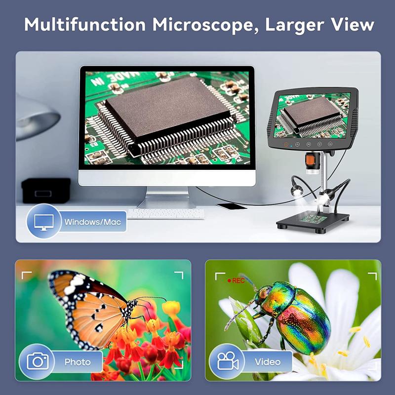
Scanning vs transmission electron microscopy
Scanning electron microscopy (SEM) and transmission electron microscopy (TEM) are two powerful techniques used to study the structure and properties of materials at the nanoscale level. Both techniques use a beam of electrons to image the sample, but they differ in the way the electrons interact with the sample.
In SEM, a focused beam of electrons is scanned across the surface of the sample, and the electrons that are scattered or emitted from the sample are detected to form an image. SEM is particularly useful for studying the surface morphology and topography of materials, as well as for analyzing the composition and distribution of elements on the surface.
In TEM, a beam of electrons is transmitted through a thin sample, and the electrons that pass through the sample are detected to form an image. TEM is particularly useful for studying the internal structure and composition of materials, as well as for analyzing defects, crystal structures, and chemical bonding.
The latest point of view is that both SEM and TEM are complementary techniques that can provide valuable information about the structure and properties of materials. In recent years, there has been a growing interest in combining SEM and TEM techniques to obtain more comprehensive information about materials. For example, a technique called scanning transmission electron microscopy (STEM) combines the high-resolution imaging capabilities of TEM with the analytical capabilities of SEM to provide detailed information about the structure, composition, and bonding of materials at the nanoscale level.
In summary, SEM and TEM are powerful techniques that can provide valuable information about the structure and properties of materials. While SEM is useful for studying surface morphology and topography, TEM is useful for studying internal structure and composition. The latest point of view is that combining SEM and TEM techniques can provide more comprehensive information about materials.










There are no comments for this blog.