What Is A Scanning Probe Microscope Used For ?
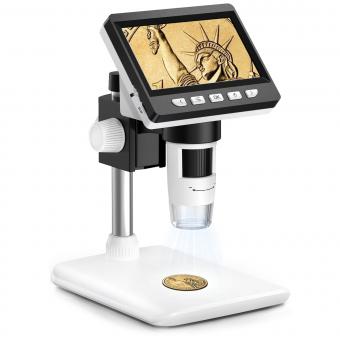
A scanning probe microscope (SPM) is a type of microscope that is used for imaging and manipulating surfaces at the nanoscale level. It uses a physical probe, typically a sharp tip, to scan the surface of a sample and gather information about its topography, composition, and properties. SPMs can provide high-resolution images with atomic-scale detail, allowing scientists to study the structure and behavior of materials at the nanoscale. In addition to imaging, SPMs can also be used for various types of surface characterization techniques, such as measuring surface forces, mapping electrical conductivity, and probing magnetic properties. The versatility of scanning probe microscopes makes them valuable tools in various fields of research, including materials science, nanotechnology, biology, and physics.
1、 Atomic resolution imaging of surfaces and nanostructures.
A scanning probe microscope (SPM) is a powerful tool used for atomic resolution imaging of surfaces and nanostructures. It allows scientists to visualize and manipulate matter at the atomic and molecular scale, providing valuable insights into the properties and behavior of materials.
SPMs work by scanning a sharp probe over the surface of a sample, measuring various interactions between the probe and the surface. These interactions can include forces such as van der Waals forces, electrostatic forces, and magnetic forces. By analyzing these interactions, SPMs can generate high-resolution images of the surface topography and other properties, such as conductivity, magnetism, and chemical composition.
The ability to achieve atomic resolution imaging is particularly valuable in fields such as materials science, nanotechnology, and surface chemistry. It allows researchers to study the arrangement and behavior of atoms and molecules on surfaces, providing crucial information for the design and development of new materials and devices.
In recent years, there have been advancements in SPM technology that have expanded its capabilities. For example, the development of non-contact SPM techniques has allowed for imaging with minimal interaction between the probe and the sample, reducing the risk of damaging delicate nanostructures. Additionally, the integration of SPM with other techniques, such as spectroscopy and manipulation capabilities, has further enhanced its versatility and utility.
Furthermore, SPMs are not limited to imaging solid surfaces. They can also be used to study biological samples, such as proteins and DNA, at the nanoscale. This has opened up new avenues for understanding biological processes and developing novel therapeutic approaches.
Overall, the scanning probe microscope is an indispensable tool for researchers seeking to explore and manipulate matter at the atomic and molecular level. Its ability to provide atomic resolution imaging of surfaces and nanostructures has revolutionized various scientific fields and continues to drive advancements in materials science, nanotechnology, and beyond.

2、 Characterization of material properties at the nanoscale.
A scanning probe microscope (SPM) is a powerful tool used for the characterization of material properties at the nanoscale. It allows scientists and researchers to investigate and understand the behavior of materials at the atomic and molecular level.
One of the primary uses of an SPM is to obtain high-resolution images of surfaces. By scanning a sharp probe over the surface of a sample, the microscope can create a detailed topographic map, revealing the surface features and structures with nanometer-scale resolution. This capability is particularly useful in fields such as nanotechnology, materials science, and biology, where understanding the surface morphology is crucial.
In addition to imaging, an SPM can also provide valuable information about various material properties. For example, it can measure the mechanical properties of a material, such as its elasticity, stiffness, and adhesion. This is done by applying a controlled force with the probe and measuring the resulting deformation or response of the material. Such mechanical characterization is essential for the development of new materials and the optimization of their performance.
Furthermore, an SPM can be used to investigate electrical and magnetic properties at the nanoscale. By attaching a conductive probe or a magnetic tip to the microscope, researchers can map the electrical conductivity or magnetic field distribution of a sample. This enables the study of phenomena like charge transport, magnetic domains, and magnetic interactions, which are crucial in fields such as electronics, spintronics, and magnetic storage.
The latest advancements in SPM technology have expanded its capabilities even further. For instance, the development of dynamic modes, such as atomic force microscopy (AFM), has allowed researchers to study dynamic processes in real-time, such as protein folding, molecular interactions, and surface reactions. Additionally, the integration of spectroscopic techniques, such as Raman spectroscopy or infrared spectroscopy, with SPM has enabled the identification and chemical analysis of materials at the nanoscale.
In summary, a scanning probe microscope is a versatile tool used for the characterization of material properties at the nanoscale. It provides high-resolution imaging, mechanical characterization, and the investigation of electrical and magnetic properties. With continuous advancements, SPMs are becoming increasingly powerful in studying dynamic processes and integrating spectroscopic techniques, opening up new possibilities for nanoscale research and applications.
3、 Manipulation and fabrication of nanostructures.
A scanning probe microscope (SPM) is a powerful tool used in nanotechnology and materials science for imaging and manipulating nanostructures at the atomic and molecular level. It allows scientists to observe and interact with matter on a scale that was previously unimaginable.
One of the primary uses of an SPM is imaging surfaces with extremely high resolution. By scanning a sharp probe over a sample, the microscope can create a detailed topographic map of the surface, revealing features as small as individual atoms. This capability has revolutionized our understanding of materials and has led to numerous discoveries in fields such as physics, chemistry, and biology.
However, the SPM's capabilities go beyond imaging. It also enables the manipulation and fabrication of nanostructures. By using the probe to exert forces on individual atoms or molecules, scientists can precisely position them to create new structures or modify existing ones. This ability has opened up exciting possibilities for nanotechnology, where the manipulation of matter at the atomic scale is crucial for developing new materials, devices, and technologies.
In recent years, there has been a growing interest in using SPMs for more than just imaging and manipulation. Researchers are exploring the potential of SPMs for studying and understanding the properties of materials, such as their electrical, magnetic, and mechanical behavior. By combining SPM with other techniques, such as spectroscopy or microscopy, scientists can gain a deeper understanding of the fundamental properties of materials and how they can be tailored for specific applications.
Furthermore, SPMs are being used in various interdisciplinary fields, such as nanomedicine and nanoelectronics, where the ability to manipulate and characterize nanostructures is crucial. For example, in nanomedicine, SPMs are used to study the interactions between nanoparticles and biological systems, which can lead to advancements in drug delivery and diagnostics.
In conclusion, a scanning probe microscope is a versatile tool that is used for imaging, manipulation, and fabrication of nanostructures. Its applications span across various scientific disciplines and hold great potential for advancing our understanding of materials and developing new technologies.

4、 Surface topography and roughness analysis.
A scanning probe microscope (SPM) is a powerful tool used for surface topography and roughness analysis. It allows researchers to investigate the surface of materials at the nanoscale level, providing detailed information about their structure and properties.
One of the primary applications of SPM is in the field of materials science. By scanning a sharp probe over the surface of a sample, the microscope can generate a three-dimensional image of the surface, revealing its topography and roughness. This information is crucial for understanding the physical and chemical properties of materials, as surface roughness can affect various phenomena such as adhesion, friction, and wear.
SPM is also widely used in nanotechnology research. It enables scientists to study and manipulate individual atoms and molecules on surfaces, paving the way for the development of new materials and devices with enhanced properties. For example, SPM can be used to investigate the self-assembly of molecules on surfaces, which is essential for the fabrication of nanoscale structures and devices.
Moreover, SPM has found applications in various fields such as biology, medicine, and environmental science. It can be used to study biological samples, such as cells and tissues, at high resolution, providing valuable insights into their structure and function. In medicine, SPM has been used to investigate the properties of biomaterials and to study the interaction between drugs and cells.
In recent years, there have been advancements in SPM technology, leading to improved capabilities and new applications. For example, the development of dynamic modes of operation, such as atomic force microscopy (AFM), has allowed for the imaging of samples in liquid environments, opening up new possibilities for studying biological systems in their native conditions. Additionally, the integration of SPM with other techniques, such as spectroscopy, has enabled researchers to obtain chemical information about the surface of materials, further enhancing the capabilities of SPM.
In conclusion, a scanning probe microscope is used for surface topography and roughness analysis. It has become an indispensable tool in materials science, nanotechnology, biology, medicine, and other fields. With ongoing advancements in technology, SPM continues to evolve, providing researchers with new insights into the nanoscale world and enabling the development of innovative materials and devices.


