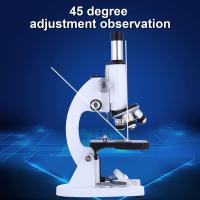
Why Scanning Electron Microscope Is Used ?
Scanning electron microscopes (SEMs) are used to produce high-resolution images of the surface of a sample. They use a beam of electrons to scan the surface of the sample, and the electrons interact with the atoms in the sample to produce a signal that is used to create an image. SEMs are particularly useful for studying the surface morphology of materials, as well as for analyzing the composition and structure of materials at the nanoscale. They are widely used in materials science, biology, and other fields where high-resolution imaging is required. SEMs can also be used to analyze the elemental composition of a sample, using techniques such as energy-dispersive X-ray spectroscopy (EDS) or wavelength-dispersive X-ray spectroscopy (WDS). Overall, SEMs are an important tool for researchers and scientists who need to study the structure and properties of materials at the nanoscale.
1、 High-resolution imaging

Scanning electron microscope (SEM) is used for high-resolution imaging because it provides a detailed view of the surface of a sample at a much higher magnification than traditional optical microscopes. SEM uses a beam of electrons to scan the surface of a sample, and the electrons interact with the atoms in the sample to produce high-resolution images.
SEM is particularly useful for studying the surface morphology of materials, such as metals, ceramics, and polymers. It can also be used to analyze the composition of a sample by detecting the backscattered electrons or X-rays emitted by the sample.
In recent years, SEM has become an essential tool in various fields, including materials science, nanotechnology, and biology. For example, in materials science, SEM is used to study the microstructure of materials and to analyze the effects of different processing techniques on the material properties. In nanotechnology, SEM is used to study the properties of nanomaterials and to develop new nanoscale devices. In biology, SEM is used to study the structure of cells and tissues and to investigate the interactions between cells and their environment.
Overall, SEM is a powerful tool for high-resolution imaging and analysis, and its applications continue to expand as new technologies and techniques are developed.
2、 Surface analysis

Scanning electron microscope (SEM) is used for surface analysis because it provides high-resolution images of the surface of a sample. SEM uses a focused beam of electrons to scan the surface of a sample, and the electrons interact with the atoms on the surface to produce an image. This allows for detailed analysis of the surface morphology, topography, and composition of the sample.
SEM is particularly useful for studying materials at the nanoscale, where traditional optical microscopes are limited by their resolution. SEM can provide images with a resolution of a few nanometers, allowing for the observation of individual atoms and molecules on the surface of a sample. This makes SEM an essential tool for researchers in fields such as materials science, nanotechnology, and biology.
In addition to its high-resolution imaging capabilities, SEM can also be used for elemental analysis and chemical mapping. By using energy-dispersive X-ray spectroscopy (EDS), SEM can identify the elements present on the surface of a sample and map their distribution. This allows for the identification of impurities, defects, and other surface features that may affect the properties of the material.
Overall, SEM is a powerful tool for surface analysis that provides detailed information about the morphology, topography, and composition of a sample. With its high-resolution imaging capabilities and ability to perform elemental analysis and chemical mapping, SEM is an essential tool for researchers in a wide range of fields.
3、 Material characterization

Scanning electron microscope (SEM) is a powerful tool used for material characterization. It is used to study the surface morphology, topography, and composition of materials at high magnification and resolution. SEM is widely used in various fields such as materials science, nanotechnology, biology, and geology.
One of the main reasons why SEM is used for material characterization is its ability to provide high-resolution images of the surface of materials. SEM can produce images with a resolution of up to 0.4 nanometers, which is much higher than that of optical microscopes. This allows researchers to study the surface features of materials in great detail, such as the size, shape, and distribution of particles, cracks, and defects.
Another reason why SEM is used for material characterization is its ability to analyze the composition of materials. SEM can be equipped with various detectors, such as energy-dispersive X-ray spectroscopy (EDS) and wavelength-dispersive X-ray spectroscopy (WDS), which can provide information about the elemental composition of materials. This is particularly useful for studying the chemical composition of materials, such as alloys, ceramics, and polymers.
In recent years, SEM has also been used for the characterization of nanomaterials. With the increasing interest in nanotechnology, SEM has become an essential tool for studying the properties of nanomaterials, such as their size, shape, and surface area. SEM can also be used to study the interactions between nanoparticles and biological systems, which is important for the development of nanomedicine.
In conclusion, SEM is a versatile tool that is widely used for material characterization. Its ability to provide high-resolution images and analyze the composition of materials makes it an essential tool for researchers in various fields. With the increasing interest in nanotechnology, SEM has become even more important for the characterization of nanomaterials.
4、 Elemental analysis

Scanning electron microscope (SEM) is used for elemental analysis because it provides high-resolution images of the surface of a sample and can also detect the elemental composition of the sample. SEM uses a focused beam of electrons to scan the surface of the sample, and the electrons interact with the atoms in the sample, producing signals that can be used to create an image of the surface. The signals produced by the electrons can also be used to determine the elemental composition of the sample.
SEM is particularly useful for elemental analysis because it can detect elements at very low concentrations, down to parts per million or even parts per billion. This makes it a valuable tool for a wide range of applications, including materials science, geology, and biology. For example, SEM can be used to analyze the composition of minerals in rocks, to study the structure of biological tissues, and to investigate the properties of new materials.
In recent years, there have been significant advances in SEM technology, including the development of new detectors that can provide even more detailed information about the elemental composition of samples. For example, energy-dispersive X-ray spectroscopy (EDS) detectors can be used to detect the X-rays produced by the interaction of the electron beam with the sample, providing information about the elemental composition of the sample at a very high spatial resolution.
Overall, SEM is a powerful tool for elemental analysis, providing high-resolution images and detailed information about the composition of samples. With continued advances in technology, SEM is likely to remain an important tool for scientific research and industrial applications in the years to come.


